A couple months ago, I wrote the first in a series of posts on an introduction to PCB Design and Manufacturing: In that post, I gave a very high-level overview of the process and began introducing some key concepts for PCB CAD design. In this post, I’ll spend more time giving details on the first part of the process: Schematic Design.
I usually describe schematic design as the part of the process where we define the logical connections in a circuit: The schematics will specify how different terminals of components are connected to each other. It’s important to bear in mind that each component shown in a schematic has a physical counterpart but that, generally, the schematic representation of the component emphasizes its function rather than its physical attributes. The physical attributes of the components will become more relevant in the next blog post when I cover PCB Layout.
To help guide our discussion on schematic design, I created the ‘Hello World’ of electronics: An LED circuit.
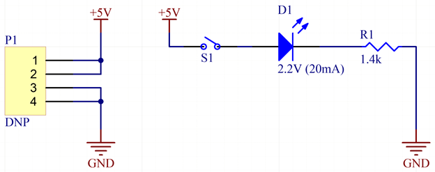
Figure 1: Schematic of an LED Circuit
This is about as simple as a circuit can get: It has one connector, a switch, an LED, and a resistor. Four components generally won’t take us very far in the world of electronics design, but they’ll be enough to demonstrate the basics of schematic design!
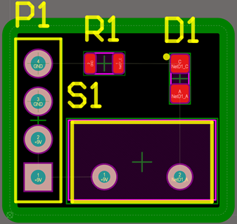
The first thing to point out are the designators. In our LED circuit, the designators are P1, S1, D1, and R1. It is imperative that each component be assigned a unique designator, otherwise, you run the risk of installing a component where it doesn’t belong.
The next thing to point out are the component values. Except for S1, all the components in the schematic have a value displayed in the schematic. The easiest component in our circuit to explain is R1: From the previous blog post, we know that the symbol for R1 is for a resistor and, from the value we see in the schematic, we know that R1 is a 1.4 kOhm resistor.
D1 is our LED. The value has two parts: First, the 2.2V indicates that the forward voltage drop across the diode is 2.2V and, second, the (20mA) indicates that the test current through the LED is 20mA; the maximum permissible LED current is typically not much more than the indicated test current, but this detail is something that should be confirmed in the component’s datasheet.
P1 is an interesting case: Normally P1 would be a 4-Pin header (like the one shown in Figure 2). However, take note of the value for P1: “DNP.” Those letters stand for “Do Not Populate,” (some people use “DNI” – “Do Not Install” – instead of DNP) and it indicates that, although the PCB is to have a place where the component could be installed, the component is to be left off.
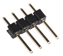
Figure 2: 4-Pin Header
There are several reasons to DNP a component. For example, some circuits allow for certain functions to be configured in hardware, but the designer may not know for sure if those functions are necessarily needed; a solution would be to place a DNP component that would allow for the option to configure the circuit in a particular way should it be determined that the functionality is needed. Another reason to DNP a component would be to illustrate what DNP means, similar to what I’ve done here.
Next things are the power rails, +5V and GND. The astute observer will note that there are two symbols in the schematic labeled +5V and two labeled GND. When it comes to power symbols like the ones shown in the schematic, it is understood that those lines are electrically connected, even though there is not a line connecting them in the schematic. In other words, I could have drawn a line from Pin 1 and Pin 2 of P1 to S1 and it would have been the same as what’s shown in the schematic – but I opted to use the power symbols to illustrate how they are used in schematics. For a circuit that’s as simple as our LED circuit, I could easily have avoided using the power symbols, but for more complex circuits, the use of power symbols becomes necessary.
It’s beyond the scope of this blog post to delve very deep into circuit design, but, for sake of completeness, we’ll go through design of my schematic example.
The first component I selected was the connector, P1. I didn’t put too much thought into the connector for this example – I just needed a way to apply power for this circuit. I picked a 4-pin DNP header for no other reason than that’s one of the first things that popped up in our component database library and it gets the job done. But it could just as easily have been a 2-pin header for this circuit or even just two plated through-holes where wires could be soldered.
I connected +5V and GND to P1 – since this is an example circuit, my decision to use +5V was arbitrary. Since +5V is a common value, I went with that.
Next, I didn’t want this circuit to just turn on the LED when power was applied to P1 – I wanted there to be some level of user control. So, I added a slide switch, S1, that would allow the user to turn the LED on and off without having to remove power from the connector.
Finally, I added the LED, D1, and the current limiting resistor, R1. The design of an LED circuit requires that 1) The voltage source be high enough to bias the LED and that 2) the current going through the LED is limited to something that won’t kill the LED.
The forward voltage across the LED is 2.2V and its test current rating is 20mA; I decided to design this circuit for 2mA, because that’s enough to turn the LED on and I’m not trying to blind anyone. With all these in consideration, I was able to design the value for R1:
- From Kirchhoff’s voltage law, the voltage drop across the resistor is .
- Since I know I want 2mA flowing in my circuit, I can use Ohm’s law to calculate the value that my current limiting resistor needs to be, .
Typically, what happens at this point in the process is a design review. This is where the designer sits down with at least one other engineer and reviews the schematics.
For our LED example, a review might start by looking at P1. Since it’s a DNP component, there isn’t too much to review. However, it does bring my attention back to that +5V rail. Although +5V is a fairly common voltage value, it might be better to assume a +9V system, so that an arguably more accessible +9V battery could be used with our circuit. If I really wanted, I could even swap P1 to specifically be a +9V battery pack connector. However, since we could just solder wires into the through holes of the DNP header, I’ll forgo the change for P1.
Next, S1 could be reviewed. The component I had selected for S1 is part number AS11CP. Reviewing the S1’s datasheet reveals that the switch is rated for 28V and for 0.4VA maximum at 28V. At the absolute worst case of +9V across the switch, this corresponds to a current rating of 44mA, well above our 2mA circuit current. Note that the only condition that the switch would see +9V is when power is connected to the PCB and the switch is OFF; however, in this scenario, there would be close to zero current flowing. Additionally, with the switch ON, the voltage drop across the switch would be negligible due to the miniscule switch resistance. In all normal case uses, the power rating of the switch is well above what we would expect it to see.
Finally, we can still use the same LED, but our current-limiting resistor will need to change now that we are assuming a +9V source. Going through the calculations again, our resistor, R1, needs to be updated to 3.4 kOhms to maintain 2mA in our circuit. Additionally, since the voltage drop across the LED will be 9-2.2 = 6.8V, and since there will be 2mA flowing through the resistor, the power dissipated in the resistor will be 6.8 x 0.002 = 13.6mW. The new resistor for our LED circuit is part number ERJ-6ENF3401V, which has a power rating of 125mW, plenty of headroom.
If we didn’t update our current limiting resistor and left it at 1.4 kOhms, we could still apply +9V to the circuit – our circuit current would just be 4.9mA instead of 2mA and our resistor would dissipate 33mW, still within an acceptable range to not blow anything up. So, we could have left R1 alone and all that would have changed is that our LED would be brighter and we’d be using more than twice the amount of power.
Our updated LED schematic is shown below:
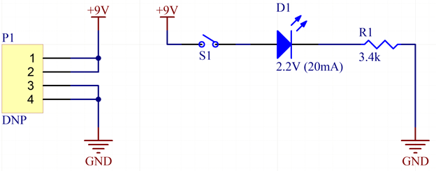
Figure 3: Revised LED Schematic
With the schematic design review done, the next step is the PCB layout. Personally, for me, PCB layout is my favorite part – it’s like a puzzle! However, that will be the topic of the next blog post. So, until then, in the closing words of my Polish Math professor from college, “All for today!” in Polish accent.