Part 1: Introduction
Once upon a time, not that long ago, I knew nothing about what goes on in getting a Printed Circuit Board (PCB) designed and assembled. There’s still a lot that I don’t know, but at least now I know the basics!
When I was initially dipping my toes in the cauldron of queso that is PCB design and manufacturing, I mostly remember being frustrated by how much trouble I was having finding answers to my novice questions. Inspired by my experiences, I decided I would write a short blog series that gives a broad-strokes overview to the world of designing and building custom circuit boards. These blog posts are, in no way, intended to be comprehensive tutorials, but rather more of an informal introduction: My hope is that they’ll help in getting beginners driving around the parking lot, but not so much around a racetrack.
The content for these posts will largely be taken from my personal experiences/anecdotal evidence and probably shouldn’t be taken as the defacto standard; but, I’ll try providing more sciencey references wherever possible.
In future installments of this series, I’ll cover topics such as schematics, board layout, and manufacturing. Before that, however, I’ll spend this blog post by, firs, giving a high-level overview of the PCB design/manufacturing process and, second, giving details on the PCB designer’s most important tool: The PCB CAD software.
PCB Design and Manufacturing Overview
Figure 1 shows a simplified PCB design and manufacturing overview.
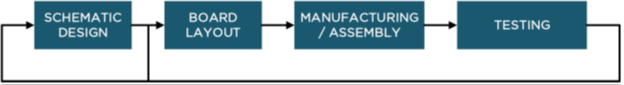
Figure 1: PCB Design and Manufacturing Process
A more complete picture of this process would show a step before SCHEMATIC DESIGN and that step would be something to the effect of SIMULATIONS; however, since this blog series has more to do with the basics of PCB design rather than the details of circuit design, I decided to ignore the work that is done prior to schematics.
This blog series will give details on the following topics:
SCHEMATIC DESIGN The schematics of a PCB show the logical connections between each component. In other words, it specifies which pins of each component need to be connected to each other. Once all the necessary connections are specified, the next step of the design process is to specify how the connections are to be physically made on a printed circuit board.
BOARD LAYOUT Once the schematic design is complete, the shape of the PCB needs to be specified, each component needs to be placed on the board, and each connection defined in the schematics needs to be made by drawing copper traces between each pin: All of this is accomplished during board layout.
MANUFACTURING / ASSEMBLY Once the board layout is complete (and everything has been reviewed and re-reviewed), manufacturing files are generated. These are the files that are sent to the fabrication house to have the board manufactured. Additionally, if the assembly of the board (soldering the components onto the PCB) is being outsourced to an assembly house, additional specifications may need to be provided to ensure that the board is assembled correctly.
TESTING Once the board is manufactured and populated with components, the final assembly needs to be tested to verify that it’s functioning correctly. Unfortunately, more often than not, the testing reveals design oversights that were not caught in the design reviews. The discoveries made in testing often necessitate revisiting the schematics, layout, or both.
With the exception of possibly Testing, each step of the design/manufacturing process requires use of the PCB CAD software. The following section gives a brief overview of CAD software and how it’s used.
Computer-aided Design (CAD)
A quick internet search will reveal that the word “cad” is dated and informal and that its definition is “a man who behaves dishonorably, especially toward a woman.” This is a different thing than what we’re talking about.
In the world of engineering, CAD stands for Computer-aided Design. Depending on the application, there are different types of CAD programs; for example, some CAD programs are strictly for designing mechanical parts and others may be for designing circuit boards.
We’re interested in the CAD programs that are geared towards circuit boards. Some examples would include EAGLE, PADS, Altium, and others. It is not uncommon for a particular CAD to have a free version available to hobbyists; not without their limitations, the free versions are generally sufficient for simple projects. In the examples that will be shown in this blog series, Altium will be used; however, instead of focusing on its features, Altium will be used primarily to illustrate different concepts. And also to show some features.
My experience is primarily with Altium, so much of what I describe will be with respect to how things are done in Altium; other CAD programs may accomplish certain things differently, but the general idea should still exist in some form.
In this blog post, I’ll give brief descriptions for some of the more important concepts in PCB CAD design.
The first concept is the idea of a schematic symbol. The schematic symbol is a representation of a component and it includes all pins of the component as well as other relevant information, such as the component’s value (for example, a resistor might have a value of 100 Ohms or a capacitor might have a value of 100 nF). An example of a resistor schematic symbol is shown in Figure 2.

Figure 2: Resistor Schematic Symbol
The 300 below the symbol indicates that the resistor is 300 Ohms; the R2 is the designator and is a unique identifier of the part – no two components in a project can have the same designator.
The second concept is the idea of a PCB footprint. The PCB footprint exists in the PCB layout view and, within the layout view, there is a 2D representation and a 3D representation; the 2D representation is primarily used for positioning the components on the board and then routing the connections. An example of a resistor footprint in the 2D view is shown in Figure 3.
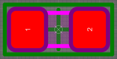
Figure 3: 2D View of a Resistor Footprint
The two red square are called pads and they represent the areas of exposed copper on the circuit board where the terminals of the resistor are connected to the board. The ‘1’ and the ‘2’ on the pads indicate the pin numbers.
Figure 4 shows the 3D view of the resistor. The blue area is the surface of the PCB and the two gold-colored squares are the pads.

Figure 4: 3D View of a Resistor Footprint
It’s not critical for designing a PCB, but more and more CADs are incorporating 3D modeling in the layout view. When creating a footprint for a given part, the designer has the option of adding the component’s 3D model; the 3D model for many components can be found online, whether directly from the manufacturer or from a third-party website that allows users to upload their own models. Like I said, it’s not a critical feature for designing PCBs, but, as a design gets more and more complex, the 3D modeling can be extremely helpful in making sure that components don’t bump into other elements of the design, such as an enclosure if the design has one.
One of the primary functions of PCB CAD is in linking the schematic symbol with its footprint. Each CAD program has it’s own way of accomplishing this – one of the ways that Altium can accomplish the linking is with a Database Library file in tandem with a spreadsheet that includes all pertinent information for a given component: The spreadsheet entry for a component specifies the schematic symbol as well as the footprint reference; the Database Library takes that information and links the two drawings together, tying pin 1 of the schematic symbol to pin 1 of the footprint, pin 2 to pin 2, etc.
Additionally, the designer can specify any other relevant information for a given component in its database spreadsheet entry. Typically, during the design process, components with specific parameters are selected and it becomes necessary to include those details in the database – these parameters may include part numbers, values, electrical ratings, tolerances, etc. Selecting parts for a design is, in itself, an art, and I’ll provide a brief introduction on that in my next blog post on schematic design.
The information I gave in this blog post barely scratches the surface of what all is involved with PCB CAD (remember: parking lot, not racetrack) – however, it is enough information to serve as a springboard for my upcoming blog posts. In my next posts, I’ll use a very simple circuit to walk through the schematic design, then the board layout, and, lastly, the manufacturing and testing process.