Introduction to PCB Design and Manufacturing Part 4: PCB Manufacturing
So, you’ve created your schematic, you’ve laid out your PCB, you’ve had multiple design reviews with your esteemed colleagues, and you’re certain that your design will work exactly as expected (haha). Now you’re ready to get the thing built!
Getting the thing built has two parts to it: First, the PCB needs to be manufactured; second, the components need to be installed on the PCB. There are two different ways to approach these tasks, but, before I get to those, I’m going to back up and spend some time on creating a DOPE manufacturing package. I’m just kidding – manufacturing packages aren’t that exciting. But, they are required.
A manufacturing package is a package that contains all files and instructions required to complete the manufacture and assembly of your project. The contents of a PCB Assembly manufacturing package may include the following items:
-
- PCB CAD Files
- PCB Specifications
- Bill of Materials (BOM)
- PCB Assembly Specifications
PCB CAD Files
The machines that fabricate printed circuit boards need instructions in their special computer language (*beep boop*). These instructions are relayed to the machines through CAD Files. All PCB CAD software should have the capability to export the PCB data from your project into some type of machine-readable CAD file.
Typically, there are two different formats for the CAD files that most PCB manufacturers will accept: Gerbers and ODB++. Gerber files are the OG format and, for most cases, will get the job done just as well as ODB++. However, if you do a simple online search-engine search for “Gerber vs ODB++,” you’ll find some information on how ODB++ may excel over Gerber. At any rate, most PCB manufacturers will accept either format.
Since each software does it differently, I won’t spend any time on the specific steps for exporting the files, only to say that there should be some option where the designer can select which layers of the PCB are exported. You’ll want to make sure all the necessary layers are selected to be exported: These layers would include all the copper layers, silkscreen layers, etc. If you forget a layer that’s needed, the fabrication house will usually catch it and contact you; relying on the fab house to catch mistakes generally isn’t the best practice, but it happens.
PCB Specification
This is a simple document that provides all design requirements for the PCB that is not explicitly captured in the CAD files. The details in this document would include things like how many copper layers the board has, how thick the board should be, what color the Soldermask should be, what the surface finish should be, etc.
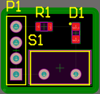
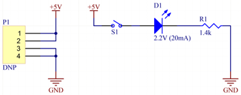
For a general-purpose circuit board (like our LED example circuit from previous blog posts), the default recommendations made by the fab house are sufficient. However, there are special cases when it would not be prudent to follow the default specifications. For example, if one of the requirements for a design is that it must remain operational at high temperatures (like the kinds of temperatures they see in drilling applications!), special considerations must be made for the construction of the circuit board. This would include things like specifying dielectric material that’s used between the copper layers to be a material rated for the expected temperatures.
Bill of Materials (BOM)
The Bill of Materials is a comprehensive list, usually in the form of a spreadsheet, of all the components to be installed on the circuit board. The BOM lists each component by its designator and specifies its part number. To make life easier, the BOM may also include brief descriptions of each component so that a quick glance at the BOM can give an idea of the types of components in the design.
In an ideal world, the person in charge of purchasing the components would be able to open up the BOM, search for each part number, find the parts stocked and ready to purchase from a reliable source (like Digi-Key, Mouser, Newark, etc.), purchase the parts, and have everything ready for assembly by the time the circuit board manufacturing is complete.
Unfortunately, we live in a world where things like “supply chain shortages” are things that happen. Lame. For simple designs, the effects of these semiconductor droughts may not be immediately noticeable; however, for more complex designs that use more parts, what often happens is that a part will be selected during the design process and by the time the design goes to manufacturing, the part will be out of stock.
When this happens, a list of “exceptions” that specifies all the parts that are out of stock is compiled. To complete the assembly process, all the exceptions must be addressed, usually by providing an alternate part number that can be used instead of the originally specified part number.
PCB Assembly Specifications
Similar to the PCB Specifications, the PCB Assembly Specifications is a document that provides all the details needed for assembling a circuit board assembly. These details may include requirements on things like the type of solder to be used, required standards of workmanship, etc.
Depending on how the board will be assembled, this document may also require drawings that show where and how each component specified in the BOM is to be installed on the PCB.
The descriptions given above for the contents of a typical manufacturing package cover most of what’s needed to get a circuit board assembly built. Of course, there may be designs that have specific requirements that may warrant additional documentation.
Once you have a suitable manufacturing package put together, you can start getting the thing built. Like I mentioned at the beginning of this post, there are two approaches to accomplishing this: Pay someone to assemble it or assemble it yourself!
In the case where you outsource the assembly to a contract manufacturer (CM), you can typically just submit the full manufacturing package and they’ll take care of ordering the boards from a fabrication house for you. Then, once they receive the boards, they’ll use the BOM and the Assembly Specifications to build the assembly to your requirements.
If the design is complex and has a lot of parts, your manufacturing package should also include a pick and place file. This file is another CAD File that can be used by the CM’s fancy robots to automatically place all the components onto the board before running the board through a soldering machine. This method of building the boards is the most expensive of the options, but, if the boards have a lot of parts and, especially if you need a lot of boards, this is practically your only option.
If the design is simple (like our example LED board!) and you have a knack for assembling small components, you can build the board yourself! In this case, you would need to purchase everything on your own, including the PCB from a fab house and all the components in the BOM. Once you have all the material, you can open up your handy-dandy Assembly Specifications drawings and get to soldering! There are different ways you can assemble a PCBA in a makeshift home-lab, but that’s a topic for a different day.
There are a lot of details and nuances that I left out in this blog series on PCB Design and Manufacturing, but such is the nature of introductions. However, after introductions, experience is the best teacher – so, get to building!