A couple months ago, I wrote the second in a series of posts on an introduction to PCB Design and Manufacturing: In that post, I covered the basics of schematic design by going through the design process for a simple LED circuit.
After the schematic has been designed and reviewed, the next step in the PCB Design and Manufacturing process can begin: PCB Layout. Personally, PCB layout is my favorite part of the process.
In Altium, each component has a schematic symbol (what we discussed in the previous post) as well as what’s known as a “Footprint.” The footprint is the representation of the physical part as it would sit on the printed circuit board. Take our LED as an example: The LED component is shown in Figure 1
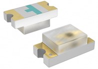
Figure 1: LED
You can see on the bottom side of the LED, there are two, gold-colored terminals that correspond to the two pins of our LED schematic symbol. To physically connect our LED in our PCB circuit, our PCB will need two pads of exposed copper that the terminals of the LED can be soldered to. An example of what this might look like in Altium is shown in Figure 2.
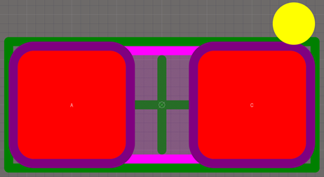
Figure 2: LED Footprint
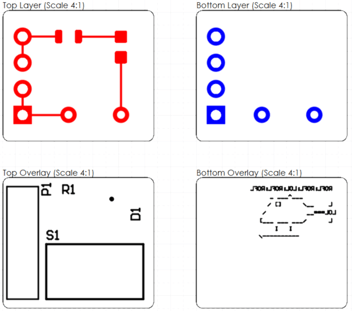
The footprint has multiple layers and each layer contains information pertaining to different attributes of the physical part:
-
- The red squares represent copper pads on the top layer of the PCB.
- The purple regions around the perimeter of the copper pads are on the Top Soldermask layer : The Soldermask of a PCB is a thin polymer layer on the surface of the PCB that covers and protects copper from oxidation and shorts. Most manufacturers allow the designer to choose the color of the Soldermask – green Soldermask happens to be the most common option (and, typically, least expensive).
Regions marked by in this layer are areas on the PCB where Solder Mask is to be omitted. It may not be obvious in Figure 2, but those purple regions extend underneath the red squares, meaning that the entirety of the pads (plus a small perimeter around the pads) are areas where Soldermask is not to be present and where the copper is to be exposed. If Soldermask was included in those areas, it would not be possible solder the LED onto its pads. - The yellow circle is on the silkscreen layer : The silkscreen is the layer of the PCB that uses ink on the surface of the board – this is the layer where the designer can add meaning markings that will be visible on the surface of the final product. For our LED footprint, the dot is next to the cathode pad and, when the LED is installed on the board, it’s cathode terminal is to be installed on this pad and the anode terminal on the other pad.
In addition to part orientation markings, other useful information that may be included on the silkscreen layer are part designators, company logos, board revision numbers, etc. Some examples of non-useful information that may be included are stick-figure people, references to hilarious internet memes or pop culture, or anything else that speaks to the designer’s personality while maintaining an acceptable level of professionality. - The green box is on the courtyard layer : In short, this layer is kind of a rule-of-thumb keep-out for the component that assists the designer in placing multiple components such that they aren’t too close to each other.
- The pink regions are on the layer that contains the part’s 3D CAD information. A lot of 3D models exist for various PCB components and Altium allows for the model to be included in the footprint – I’ll cover the Altium’s 3D view later in this post.
- There are other layers, but the ones mentioned here are the most important.
- The red squares represent copper pads on the top layer of the PCB.
The footprint specifications for a given part (e.g. the dimensions of the pads, the spacing between the pads, etc.) are typically provided in the part’s datasheet. However, many parts (not all) follow a standard footprint package, so the designer does not need to worry about verifying the dimensions of the footprint every time a different part is used, provided that the package is identical.
The LED in our example is an 0805 package – if I later decided that I wanted to use an LED with a different color, I could easily just find another 0805 LED and make the substitution (I might have to update the value of my current-limiting resistor, but, since a resistor like that would have a standard package, that would also be an easy substitution to make).
At this point, we’ve covered the two CAD elements for a component, its schematic symbol and its PCB footprint. There’s more to be said about how Altium joins these two elements together and how the pin-mapping happens (i.e. how each schematic symbol pins are mapped to their corresponding footprint pads); however, those details are beyond the scope of this blog post – suffice it to say that, before a component can be used in a project, its schematic symbol needs to be linked to its footprint.
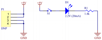
With the schematic completed, we can update our project and push all the components specified in the schematic into our PCB Document. Figure 3 is the first thing we see after pushing our circuit to the PCB document: The components of our LED circuit can be seen on the right and the PCB itself is on the left (the particular shape of the board shown in Figure 3 is just a remnant from a previous project).
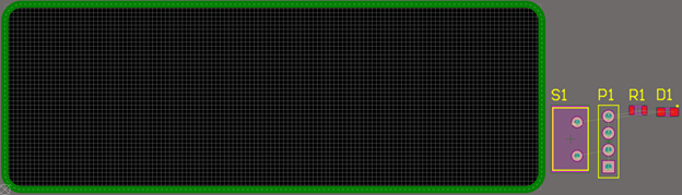
Figure 3: PCB Layout - Initial 2D View
Taking a closer look at our components (Figure 4), notice the thin lines connecting the pads of the components. These airwires, or ratsnest, show the logical connections that are defined in our schematic. The airwires will be critical in assisting how we place our components on the PCB such that our wired connections flow efficiently.
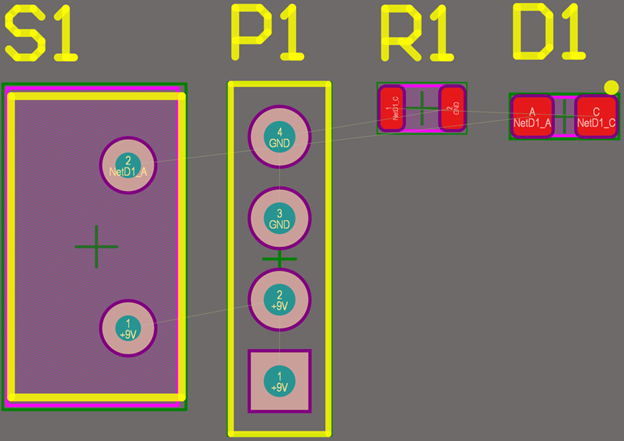
Figure 4: PCB Layout – Airwires
Before we begin making any connections (or, routing), we need to position the components on the board. Arguably, the majority of PCB layout is spent placing the components in a way that makes the routing process easiest – if the component placement is good, the routing should be quick and painless!
However, before placing the components, I think the board shape in Figure 3 is a little too big for our small circuit. Switching to the Board Planning Mode in Altium, I can redefine the board shape to something a little more appropriate for my circuit. Depending on the design, determining the board shape might need to be an iterative process, but I like to have a ballpark shape to work with when I begin placing the components.
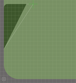
Figure 5: Board Planning Mode | Left - Redefining Board Shape, Right - New Board Shape
Switching back to the 2D Layout view, the components can be placed with the help of the airwires; Figure 6 shows how the components have been placed in a way where the airwires follow a simple square pattern, from P1:Pin 1 to S1:Pin 1; then from S1:Pin 2 to D1:Pin A, etc.
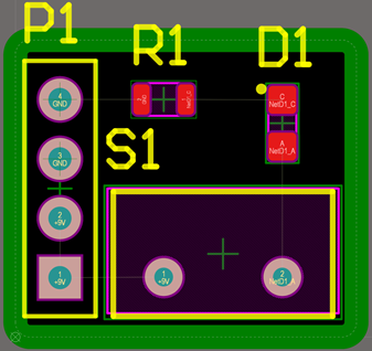
Figure 6: PCB Layout - Component Placement
With the components positioned on the PCB, Altium’s interactive routing mode can then be used to define how copper traces connect the pins; the airwires disappear as each connection is routed; the left image in Figure 7 shows how the interactive routing uses the airwires to assist the designer in placing copper traces between pads and the right image in Figure 7 shows the completed routing of the board.
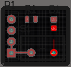
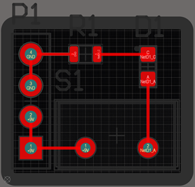
Figure 7: PCB Layout, Interactive Routing
With the routing complete, the PCB just needs to be cleaned up and prepared for a design review. Since this design is so simple, this task will only involve resizing and repositioning the silkscreen designators.
Remember how I mentioned that Altium allows for a component’s 3D model to be embedded? Figure 8 shows the 3D models in action when I switch to Altium’s 3D View of the completed board. It’s looking pretty pretty pretty good.
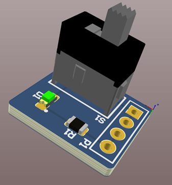
Figure 8: PCB Layout - 3D View of Completed Board
There’s a whole lot of stuff that I did not cover due to “I don’t want, nor am I qualified, to write an entire novel on this topic.” Keep in mind that the purpose of this blog post is to give a very basic introduction to the world of PCB design. To that effect, I opted to not discuss several key concepts, such as board stackup, vias, copper pours and planes, how to select appropriate trace widths, running the Design Rule Check, and the list goes on.
As a matter of fact, I didn’t even cover what a design review for a board layout would look like…it probably would have caught the fact that I didn’t add any silkscreen labels for the connector that would have made it abundantly clear on how power needs to be connected. The design review would have also probably scored a round of high-fives when the silkscreen ROFLCOPTER that I added to the bottom side of board was discovered.
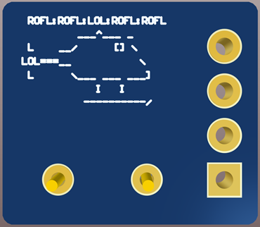
Figure 9: lol.
The next blog post in this series will be the final post of the series: It’ll cover the basics getting a board manufactured! Until then, I’ll PCB you later!